
Firmware Architecture#
At a high level, the firmware is organized into functional modules responsible for signal processing, acquisition, timing, and board interfacing. The architecture combines acquisition, waveform generation, trigger handling, and board-specific integration into a cohesive RFSoC datapath.
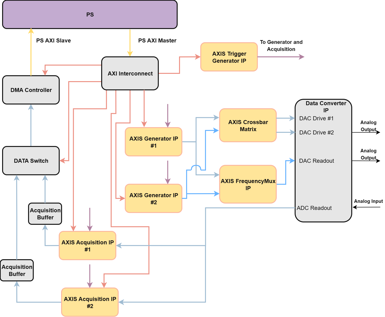
Architectural view#
The firmware is composed of several IP blocks that interact through AXI and AXI stream interfaces:
The PS block exposes the PL-PS communication interfaces, indicated using the yellow AXI Master and Slave ports.
The AXI Interconnect block is an AMD IP (all AMD IPs are in gray) providing AXI connectivity between a single master and multiple slaves, represented by the red connections.
The Acquisition Buffers store data transferred to them via the AXI Streams (represented by the blue connections) that are used to as temporary storage for the experiment results and provide enough storage to run many shots one after the other.
The Data Switch allows to select one of the two buffers for data extraction.
The Data Converter IP is a special IP that provides configuration and communication with the dedicated RF data converters included in the PL.
Custom IP#
The Acquisition block receives samples from the ADCs and produces demodulated and decimated (or accumulated) streams.
The Generator block produces the drive and readout waveforms used by the experiment flow.
The Trigger generator coordinates timing and dispatches trigger words to the other blocks (represented by the violet connections).
The Frequency Multiplexer aggregates multiple tone streams, each corresponding to a distinct resonator frequency, into a single output stream. This enables the readout of multiple qubits through a single physical line.
The Crossbar Matrix provides flexible connectivity between generators and DACs, enabled for drive pulses.